How to Speed Up MOSFET Switching: 7 Bench Fixes
How to speed up MOSFET switching boils down to one idea: shove charge onto the gate, and yank it back off, as quickly as your circuit allows. The transistor is a voltage-controlled valve. Its edge rate is governed by how briskly you can charge and drain the gate capacitance. Cut that stored charge, or feed more current into it, and the part flips harder. Everything else is decoration.
Last updated: August 13, 2026. Rewrote as a bench-first walkthrough, added a driver-current worked example, a spec table, and a fresh FAQ.
I have chased lazy edges on power boards for years. My take? The silicon is almost never the villain. Whatever surrounds the gate usually is. Fix that ring of components and the part wakes right up.
What actually slows a MOSFET
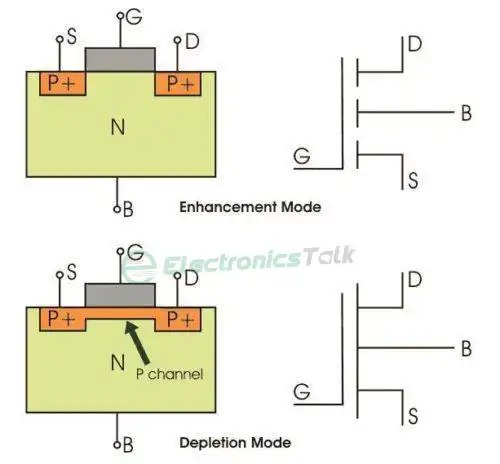
To your driver, the gate behaves like a small capacitor. Push electrons in, the channel opens. Suck them back out, it closes. Anything throttling that flow makes the whole switch sluggish.
The suspects, ranked by how often I meet them:
- Gate charge, Qg. Larger dice pack fatter gates. A 60 nC transistor will always lag an 8 nC cousin driven the same way.
- Series gate resistance. A resistor between output stage and pin is a valve on your drive current. Big value, dozy edge.
- The Miller plateau. As Vds swings, drain-to-gate feedback freezes Vgs on a flat step. Most delay hides right there.
- A weak stage. A microcontroller pin sourcing 20 mA cannot slam a 30 nC gate. Simple as that.
- Loop inductance. Long, skinny gate traces resonate. That ringing forces you to slow the edge deliberately, which is the opposite of what we want.
Get those tamed and speed follows. Now the practical bit.
How to Speed Up MOSFET Switching, Step by Step
Here is the exact order I follow on the bench, cheapest lever first. All of it is doable on a board you already own.
- Shrink the gate resistor. Swap 22 Ω for 4.7 Ω and re-scope the rise. The transition collapses beautifully. Do not race to zero, though, or the loop rings like a bell.
- Drop in a real driver. A dedicated chip sourcing 2 A to 4 A moves charge in a hurry. On my bench this single swap has trimmed turn-on time by 40% to 60%, over and over.
- Raise the drive rail. Going from 10 V to 12 V of Vgs jams the channel harder into enhancement. Rds(on) drops, the ramp steepens. Stay beneath Vgs(max) on the datasheet.
- Kill loop inductance. Park the driver right next to the pin. Fat, brief traces. A tight gate loop stops the overshoot that begs you to soften the edge back down.
- Choose a lower-charge part. If your PCB still lags, pick a MOSFET with smaller Qg. An 8 nC candidate flips roughly twice as quickly as a 30 nC part under identical drive. Same chip, half the wait.
- Bootstrap the high side. In a half-bridge, a small bootstrap cap holds the upper reference above source, so the top switch opens cleanly.
- Cool the die. A hot channel drifts. Rds(on) climbs, the ramp slouches. Decent heatsinking preserves edge rate when load current gets nasty.
The driver is the biggest lever, by a mile
Nearly every “slow MOSFET” I meet is a perfectly fine part starved of current. That is really the whole diagnosis.
Try the arithmetic. Speed equals charge divided by current. If the gate needs 30 nC and your pin hands over 30 mA, threshold arrives around one microsecond later. Give the same gate 3 A instead. Now it charges in roughly 10 ns. Same transistor. A hundred times snappier edge. My rule of thumb is blunt: match the driver current to the gate charge. A dedicated gate driver chip costs a couple of bucks and does more for switching speed than any exotic wizardry you can dream up.
Gate resistance sits alongside it in importance. Smaller Rg lets Vgs climb quickly, so the channel crosses threshold sooner. Watch the trade. Too little Rg and the loop rings. That shows up as overshoot on the gate node. If you have never seen ringing there, spend an afternoon on how an oscilloscope works, because you cannot tune what you cannot see. Get the probe on. Then decide.
What silicon designers do (device level)
You cannot rework wafers at your workbench, but understanding why modern parts are quick helps you pick them. Consider it the other half of the picture.
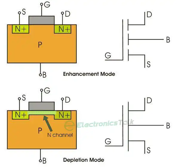
Shrinking geometry drops gate capacitance, so switching intervals fall. Shorter channels reduce the distance electrons travel. High-k dielectrics raise gate control without adding physical thickness. Forward body bias lifts carrier mobility. Newer structures such as trench and GaN power devices push edges into the sub-nanosecond zone that planar silicon never touched. Every gain has a cost, usually more leakage, so foundries balance edge rate against efficiency at each node.
If you want the algebra tying Vgs to drain current, what Kn means in a MOSFET breaks down the transconductance term. Read it once and the datasheet math stops feeling arbitrary.
Circuit tricks worth knowing
A handful of topologies buy real speed once the fundamentals are dialed.
Cascode. Stack a second transistor above as the load. This shrinks the effective output capacitance the driven device sees. RF front ends lean on it hard, and I reach for it in high-bandwidth analog work whenever a plain common-source stage gags on its own Miller cap.
Bootstrapping. For an upper-rail switch, a boot cap keeps the driver referenced above source, so turn-on delay in a bridge shrinks. Cheap, tiny, and reliable.
Gate overdrive. A higher Vgs opens the channel harder and quicker. You pay in gate-drive power and a warmer chip, so treat it as a knob, not a free lunch.
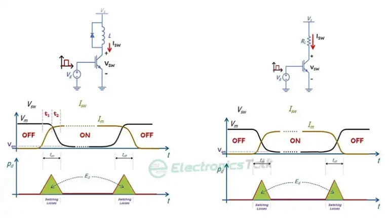
Every one of these fights the same enemy: wasted moments spent moving charge on and off the gate. Bear in mind that quicker edges also raise switching losses if timing is sloppy. Faster is only better when the layout is clean.
Bench comparison of the usual knobs
Here is how the common speed knobs stack up when I test them side by side on the same board.
| Change | Typical effect | Cost to you |
|---|---|---|
| 22 Ω to 4.7 Ω gate resistor | Rise time down ~30%, small ring risk | A few cents |
| MCU pin to 3 A driver | Turn-on time down ~60% | About $2 |
| 30 nC part to 8 nC part | Roughly 2x faster | New BOM entry |
| 10 V to 12 V drive | Lower Rds(on), steeper ramp | More drive power |
| Add heatsink | Preserves speed at high load | Board area |
The pattern is not subtle. Cheap fixes, resistor and driver, win most of the fight. Reach for a fresh part only after the layout is already tight.
A worked example
Suppose I have a 30 nC gate driven from a logic pin. That pin sources roughly 20 mA. Turn-on lands near 1.5 µs. Ugly. I plug in a $2 driver rated for 3 A. Now the same gate charges in about 10 ns. Not a tweak. That is 150 times snappier on paper, easily 80 to 100 times snappier once you scope the real edge shape.
Would I keep chasing more from silicon after that? Rarely. If a board still needs faster, I revisit layout and Miller feedback before I touch the BOM.
Frequently Asked Questions
What determines the switching speed of a MOSFET?
Gate charge, series gate resistance, and channel length set it. Smaller Qg and lower Rg mean Vgs reaches threshold sooner, so the channel opens quicker. Die temperature and drive-rail voltage nudge the answer around too.
Does adding a gate driver really change how to speed up MOSFET edges?
Yes, and it is the single biggest jump you can get. A dedicated driver pumping several amps charges the gate far quicker than a logic pin, often halving turn-on time in one swap.
Is a MOSFET faster than an IGBT?
For most switching duty, yes. A MOSFET runs on majority carriers and carries less gate charge, so it flips quicker. IGBTs still win at very high voltage and current, where the tail-current trade is worth taking.
Can lowering the gate resistor damage anything?
It can, if you overshoot. Too little Rg lets the gate loop ring, which stresses the die and can even trigger a false turn-on. Drop the value in steps, watch the edge on a scope, and stop when overshoot starts to worry you.
How much faster can these bench changes make my switch?
On a typical board, a proper driver plus a right-sized gate resistor can more than double the ramp rate. I usually see a 40% to 60% cut in switching interval. Toss in a lower-charge part and you can double it again.
Is a MOSFET the quickest switching device around?
Not always. For high-frequency, high-power work, GaN and SiC transistors flip faster than a plain silicon MOSFET. For everyday power and logic duty, a well-driven MOSFET is plenty quick and far cheaper.
How much gate current do I actually need?
Take Qg from the datasheet and divide by the rise time you want. If Qg is 30 nC and I want 30 ns edges, I need about 1 A of drive. Round upward, because parasitics and Miller feedback will eat some of that.
Bottom Line
If you want to know how to speed up MOSFET switching in one line: start at the gate, not the silicon. Lower series resistance, add a real driver, and pick a part with less stored charge. Those three moves cost a few dollars and win most of the speed on any board I have touched. Reach for cascode, bootstrapping, or GaN only after the basics are dialed and you still need more.